Successive Approximation ADCs - Theory and Parameters
I have a (possibly extremely ambitious goal) of designing and taping out a basic successive approximation register (SAR) analog to digital converter (ADC) over the course of the next few months. I’m very much in the process of learning how to do this, so the posts here should just reflect me learning how all of it works, basically just collections of my notes. Hopefully most of the things I write should be correct, but corrections might be in order later down the line.
To start out, what is a SAR ADC and why should we use it? The basic goal of an ADC is to take an analog signal and convert it to a format that a computer can use, allowing us to carry out powerful operations provided by digital computing (ie DSP/Machine Learning/Controls). The SAR ADC does this by first comparing the input signal to a reference signal, feeding the result (1 or 0/VCC or GND) to a register, the register passes its value to a digital to analog converter (DAC), then we take the DAC output and comparing the input signal to that result.
Explaining this in words generally doesn’t make much sense, so here’s a good diagram (from https://www.electronics-tutorial.net/analog-integrated-circuits/data-converters/successive-approximation-type-adc/).
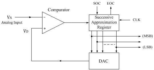
The important things to note are the output of the comparator and the value present in the register Suppose VCC is 5V, so our max output is 5V. For simplicity assume 5 bits (so 11111 output is 5V, 00000 is 0V). Let our input signal be 4V. At the 0th iteration (signal has not even been sampled yet) the register contains a binary 10000. This value corresponds to a voltage of 2.5V (if this isn’t clear review binary counting, 10000 is half of 11111). We then compare 4V to 2.5V. Since 4>2.5 the output of the comparator is again a 1. The register now holds 11000. The DAC converts this to a voltage of 3.75 volts. This comparison gives us yet another 1. The register now has 11100. This gives a DAC output of 4.375V. The comparison now yields a 0. The important part here is we flip the 3rd and 2nd bit, so we go from 11100 to 11010. This will still give us 0 since 11010 = 4.06V in our 5 bit DAC with a 5V supply voltage. So now we flip the 4th and 5th bits, giving 11001, or 3.90V. Now we see will just constantly oscillate around 3.90V and 4.06V, so our conversion is complete. This also implies our ADC has limited resolution, and of course it does, it only has 5 bits!
Off of 5 volts the maximum resolution of 5 bits is given by 5V/2^5, or 156mV, not very good, but that’s the price that must be paid for low bit count because, as will be seen when I start designing, complexity, power, and chip area all scale very much with bit count.
One more interesting thing to note is that the SAR ADC is a hardware implementation of a binary search algorithm (this fact is actually what made me want to design one). Hardware implementations of traditionally software algorithims is an exciting and rich field. There are tons of research groups/companies looking into ML accelerators for example. A series of posts on that could be interesting in the future.
Now that the basic conversion process is clear (at a high level) we should probably spec our ADC to be designed. So what are the important parameters of an ADC? Well let’s list them:
-
The first, and most obvious, is probably the bit number, or resolution. How many levels can our ADC represent digitally?
-
The sample rate. How quickly is our ADC looking at the signal, and converting it? This is determined by the fastest signal you expect to be looking at. Nyquist tells us we have to sample at at least twice the highest frequency signal in our sampled signal to completely reconstruct the sampled signal. While this is true, one gets far better results by going around 10X faster.
-
Power draw in watts
-
Signal to Noise and Distortion Ratio (SNDR) - A very important spec that is defined as the ratio of the power of a fundamental tone (say a sine wave at 1 MHz) to the sum of the noise power across some bandwidth (noise is usally defined as watt/hz) and distortion power. Distortion power is the power of signals that are not your fundamental tone, ie any frequency not at 1MHz for our sine wave example. As a matter of fact, these signals will be at integer multiples of 1MHz, called harmonics, so there will be some power at 2MHz, 3MHz, etc. We usually take the sum of the first 3 harmonics and use that as our distortion power. This page has a more intuitive explanation of distortion https://www.setra.com/blog/what-is-total-harmonic-distortion.
-
ENOB - Effective number of bits. Unfortunately our ADC will not be perfect. We will lose some resolution to noise and distortion in the system. ENOB can be computed as

The source for this equation is normally derived in an undergraduate electronics class, so I’ll skip it. This website goes through the derivation: https://www.edn.com/what-does-the-adc-snr-mean/.
There are more specs, but they’re pretty much all related to those above. So what should we shoot for? Some of the best ADC’s created are generally published in ISSCC, so looking at the data converters section for the past few years, and backing off what the average seems to be by 20% seems reasonable. I think it would be reasonable to shoot for a 30MS/s 10 bit, with a SNDR of 50dB, so an ENOB of about 8 bits. We’d like to keep the power draw low as well, less than 100mW should be achievable. This would correspond to 2.7pJ/conversion (energy per conversion is generally how ADC’s are compared). While this system absolutely won’t get into any conferences it should be very good from a learning perspective.