Who Cares About Silicon Photonics?
An emerging technology that has a lot of potential is silicon photonics (SiP). Over the past few years various foundries (Global Foundries, IHP) have released photonic PDKs, or process development kits. A PDK is what a microelectronic circuit designer uses to design circuits, it’s the set of layout rules, device models, simulation data, etc that one uses when designing a circuit. The fact that these companies have released a PDK, and are currently fabbing SiP circuits implies they expect the market to rise dramatically in the coming years, but why?
Before getting into dirty details about what one can build, it’s worth thinking about what might be worth building. One could build things like processors, sensors, communication systems, or whatever else you could think of. People have built processors that can carry out things like Hilbert or Fourier Transforms very easily but the material system is not compatible with silicon (which we want because silicon is cheap), and the amount of overhead in switching between the electrical domain and the photonic domain implies one might as well stay in the electronic domain and use digital CMOS, so photonic processors probably have quite a ways to go before they’re generally useful.
Sensors can obviously be built, LIDAR is a well known application of SiP technology, and is obviously a huge market for automotive applications like self driving, though Tesla ditched the LIDAR, and just uses cameras. (As an aside, the reason for this is interesting. Tesla found that every time the cameras and the radar/lidar/IMU disagreed, they just used the camera data as the input to their neural net. This leads to the conclusion that one can effectively do away with the auxillary systems.)
The real meat of SiP is in communication, both short distance and long distance. Server farms transmit data between compute units photonically, fiber optics is photonic, soon most satellite comm systems will be photonic. Transmitting information optically is generally just superior to doing it electronically. A multimode fiber can transmit information electronically with loss as low as 3dB/kilometer. This is about 4 times better than an extremely high performing electromagnetic wave link (2.4GHz, 60dB TX gain, 30 dB RX gain, free space path loss), and we haven’t even considered data rates yet (they’re higher). Comparing free space optics to free space electromagnetics yields a similar result.
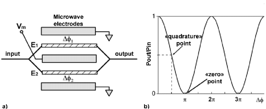
So photonics are useful for comm, where does the silicon come in? Well for a transmitter to work, one requires a modulator, and with silicon photonic integration one can build a CMOS modulator, modulating a constant light source with cheap electronics, placing a data signal on top of the optical carrier wave. The basic topology that does this is called a Mach-Zehdner modulator (MZM. While the specifics of the physical modulation mechanism vary by technology node, the basic idea is an electric field can serve to change the index of refraction of a material, and therefore change the phase of the signal passing through it. This allows for a phase modulation based scheme like QPSK to be easily implemented (though people usually use PAM-4 for photonic links). A simple schematic of a MZM can be seen below. source
The reciever block is simply a photodiode, possbily followed by an amplifier. Since we now are in the electronic domain, we can simply directly sample the recieved signal (probably after some filtering to do away with the carrier). After the ADC one just requires a DSP to retrieve the data signal, so no painful circuitry, just algorithms. A block diagram and more thorough explanation can be found here.
The jist of the idea is we can build both modulators and amplifiers (light intensity can be changed) in a silicon process. The mixture of photonic components such as waveguides, photodiodes, MZMs, combiners, etc with silicon CMOS allows for cheap integration, and will likely explode commercially over the course of the next few years.